C2S Initiative at ACEIT Jaipur
The department of Electronics and Communication Engineering received C2S approval for the EDA tools access under C2S Program, MEITY Government of India.
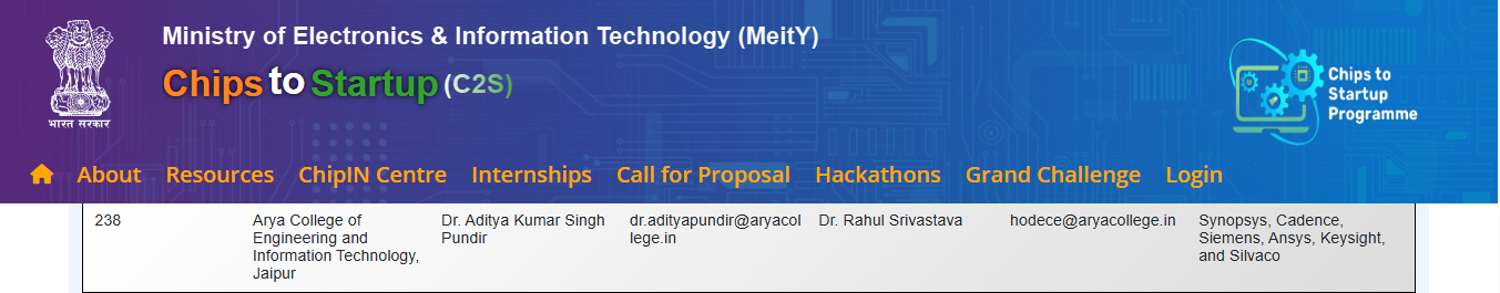
The following academics licenses of EDA tools have been provided for research and development in the field of VLSI, Semiconductor and Embedded Systems:
Synopsys, Cadence, Siemens, Ansys, Keysight, and Silvaco
The program is supported by Ministry of Electronics and Information Technology and ChipIn centre at CDAC. This initiative enables the students and researchers to access the world-class design tools, fostering innovation in semiconductor, VLSI and Embedded systems with the streamline with India semiconductor mission.
About Chips to Startup (C2S) Program
Overarching Vision: To catalyze a vibrant ecosystem for electronics system design and manufacturing in India by connecting academia, research, and industry to transform innovative ideas into commercial products and successful startups.
Core Mission: The C2S program is a comprehensive initiative designed to nurture India's electronics value chain. It achieves this by developing specialized talent in VLSI and Embedded System Design, fostering the creation of intellectual property (IP), and guiding the development of application-oriented hardware solutions through to deployment, all while leveraging and strengthening domestic Start-ups and MSMEs.
Key Objectives & Strategic Pillars:
The program's objectives are structured around four interconnected pillars:
1. Specialized Human Capital Development:
- Goal: To create a industry-ready workforce with advanced skills in VLSI design, verification, embedded systems, and FPGA/ASIC implementation.
- Action: Develop and deliver targeted training modules, workshops, and hands-on projects within academia and R&D institutions to bridge the skill gap between theory and industry practice.
2. Intellectual Property (IP) Creation and Curation:
- Goal: To build a strategic national asset and reduce dependency on foreign IP cores.
- Action: Incentivize and fund the development of a repository of reusable, open-source or licensable IPs (e.g., processor cores, interface controllers, analog blocks) created by academia and partner R&D organizations.
3. Productization and Deployment:
- Goal: To move beyond theoretical design to functional, market-ready systems.
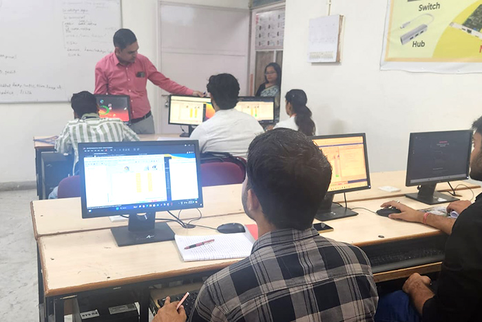
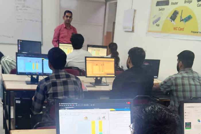
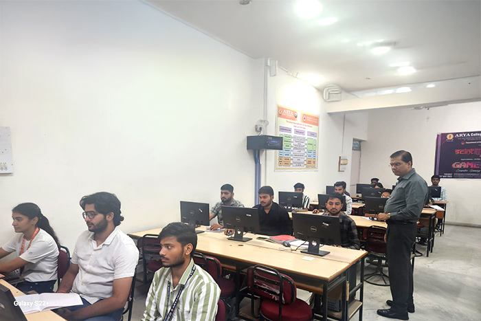
- Action: Provide end-to-end support for the design, prototyping, and testing of application-oriented systems, ASICs, and FPGAs. This includes access to EDA tools, fabrication support, and mentorship on productization challenges.
4. Industry-Academia Synergy and Commercialization:
- Goal: To ensure innovation is market-driven and creates commercial value.
- Action: Actively facilitate partnerships between academic/R&D teams and domestic Start-ups/MSMEs. This allows students and researchers to gain real-world experience while Start-ups gain access to cutting-edge innovation, creating a pipeline for new ventures and economic growth.
Activities under C2S Program at Arya College of Engineering and Information Technology Program Running:
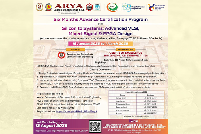
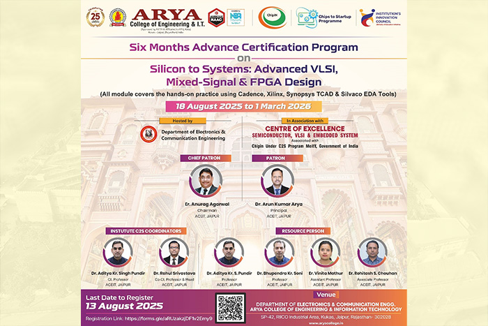
Six-Month Advanced Certification Program Silicon to Systems: Advanced VLSI, Mixed-Signal & FPGA Design
with Three Different Certification Modules:
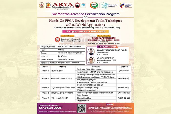
A. Hands-On FPGA Development: Tools, Techniques & Real World Applications
Tools: Xilinx ISE/Vivado
Focus: Real-world applications, prototyping, and verification techniques.
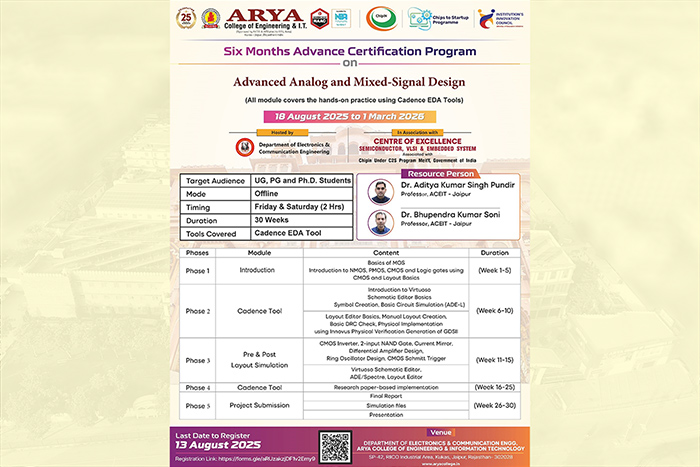
B. Advanced Analog & Mixed-Signal Design
Tools: Cadence EDA
Focus: Circuit simulation, layout design, and signal integrity analysis.
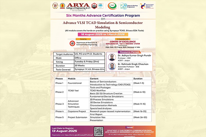
C. Advanced VLSI TCAD Simulation & Semiconductor Modeling
Tools: Synopsys TCAD, Silvaco EDA
Focus: Device modeling, process simulation, and semiconductor physics.
Course Outcomes:
- Design & simulate mixed-signal ICs using Cadence Virtuoso (schematic, layout, DRC/LVS) for analog/digital integration.
- Implement FPGA systems with Xilinx Vivado/Vitis (RTL synthesis, HLS, timing closure) for hardware acceleration.
- Model semiconductor devices using Synopsys TCAD (Sentaurus) for process optimization and device behavior analysis.
- Verify ASIC/FPGA designs using industry-standard methods (SPICE, mixed-signal simulation, formal verification).
- Execute a full RTL-to-GDSII flow (Cadence Innovus) and FPGA prototyping (Xilinx) with hands-on projects.
Registration Fee: No Fee
Venue: Department of Electronics & Communication Engineering, Arya College of Engineering and Information Technology, SP-42, RIICO Industrial Area, Kukas, Jaipur, Rajasthan- 302028
Last date to register: 10 August 2025
Joining Link: https://forms.gle/aRUzakzjDF1v2Emy9
For any further information contact:
Institute C2S Coordinators:
Chief Investigator (CI)
Dr. Aditya Kumar Singh Pundir
Co-Chief Investigator (CI)
Dr. Rahul Srivastava


 9314881683 | 9829017324
 0141-6604555 (30 Lines)
  info@aryacollege.in